Tech partner, execution of bailout plan hold key to SCL’s future
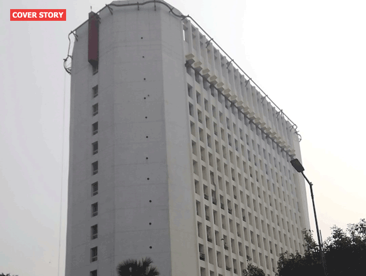
On a searing hot day in Mohali, passing through the top floor of Semi-Conductor Laboratory’s (SCL) three-tier fabrication building is a refreshing experience as it houses the air circulation system. On the first floor are all the equipment and machines, while the ground floor has utilities such as ultrapure water pipelines and management system, gas pipes, as well as chemical delivery systems.
It takes 450 steps starting from getting a raw wafer, performing cleaning steps and complex processes for multiple chips on the wafer, till the wafer goes for packaging and assembly. The process involves patterning or lithography on the wafer, which means passing chip design onto the wafer for defining circuits after which they are cleaned and polished.
More in IT